The Field Engineer in the Seismically Quiet Room#
In late 2023, ASML completed the first shipment of its High-NA EUV system — the TWINSCAN EXE:5000 — to Intel's development fabrication facility in Hillsboro, Oregon. The tool weighs approximately 150 tonnes. Installation required dismantling part of the fab building's exterior wall to admit components that could not fit through standard cleanroom access routes. The vibration isolation system beneath the tool's foundation pad is engineered to attenuate ground motion across the frequency range 0.1–100 Hz to a level below approximately 1nm/s — because any ground vibration above this threshold will couple into the projection optical system and appear as overlay registration error in the exposed features.
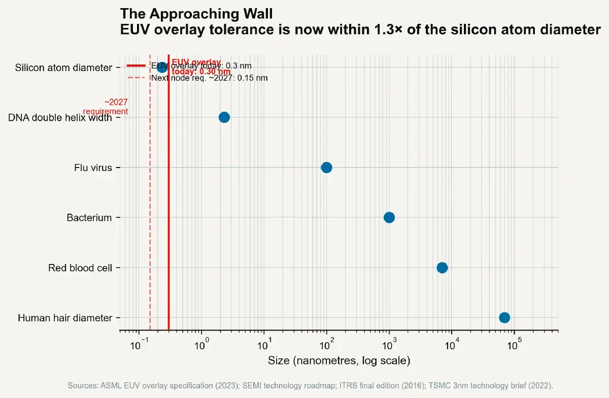
The Hillsboro site sits approximately four kilometres from the MAX light rail line. The low-frequency vibration signature of a passing train is detectable at the tool's seismic sensors and must be filtered from the active vibration isolation feed-forward control. Intel's process integration engineers, characterising the tool's overlay performance in February 2024, mapped a systematic 0.3nm overlay contribution that correlated with time-of-day — later traced to ground vibration pattern changes from the morning versus evening rail traffic schedule. The tool was achieving overlay registration of approximately ±1.7nm across the wafer field. Its successor — the EXE:5200, scheduled for production delivery in the late 2020s — targets ±1.0nm overlay. That target requires the tool's eight projection mirror surfaces to be controlled to approximately ±50pm (picometres). Fifty picometres is approximately one-quarter of the diameter of a silicon atom.
The Tolerance That Cannot Be Bought#
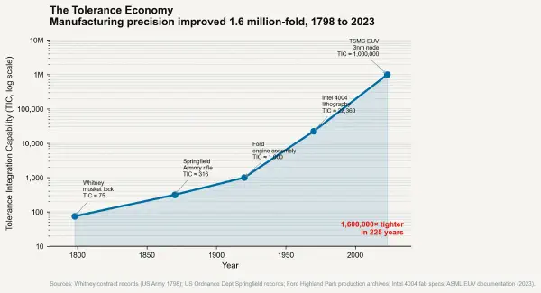
There is a category of manufacturing tolerance problem that transcends capital investment. Whitney's musket problem and Ford's assembly-line problem were ultimately solved by deploying sufficient capital to better machines, better gauges, and better process control. The semiconductor precision challenge at 2nm and below is approaching a different category — one where the limiting constraint is not underfunded infrastructure but the physics of measurement at atomic scales. The Tolerance Integration Complexity (TIC) of leading-edge semiconductor production has reached a level where each incremental improvement requires not merely more capital but genuinely new physical principles, and where the concentration of the supplier ecosystem that delivers those improvements is without precedent in the history of industrial production.
Inside the High-NA EUV Wall#
The Numerical Aperture Ceiling and What It Costs#
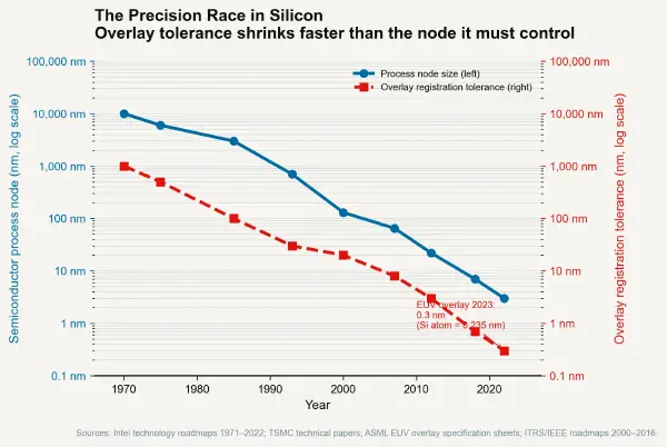
The resolution limit of an EUV exposure system — maintaining the Rayleigh criterion minimum feature = k₁ × (λ / NA) — can be improved by increasing the numerical aperture (NA) of the projection optics alongside the short EUV wavelength. The current production NXE:3600D operates at NA=0.33. The EXE:5000 High-NA system operates at NA=0.55 — a factor of 1.67 increase that reduces the diffraction-limited feature size by the same factor, enabling single-exposure patterning of features approximately 8–10nm in pitch that would require multi-patterning at NA=0.33.
Increasing NA from 0.33 to 0.55 requires increasing the diameter of the final projection mirror — the mirror closest to the wafer — from approximately 25cm to approximately 55cm. A 55cm EUV mirror polished to ±0.05nm surface roughness across its full aperture at the tolerances required for EUV projection optics is at the physical edge of what ion beam figuring technology can achieve. The manufacturing process for a single EXE:5000 projection optics set at Carl Zeiss SMT requires approximately three years from raw glass blank to qualified optical assembly. The total optical metrology infrastructure required to characterise a 55cm EUV mirror at ±0.05nm — including EUV wavefront sensors, at-wavelength interferometers, and temperature-stabilised metrology labs — represents a capital investment measurable in hundreds of millions of euros.
The economic consequence for the semiconductor roadmap is unambiguous. Intel, TSMC, and Samsung — the three companies capable of fabricating at the leading edge — must absorb development costs per new node exceeding $1 billion before first wafer yields are achieved. ASML's EXE:5000 capital cost per unit is estimated by analysts at approximately $350–400 million per tool. At NA=0.55 and with High-NA EUV, the 2nm node is achievable for approximately 4–6 exposure layers using single-exposure — with a corresponding TIC improvement over the multi-patterning approach. But the capital intensity and supply chain concentration required to access this TIC level ensures that the number of companies capable of participating approaches a minimum.
The Mirror Polished to 50 Picometres#
Carl Zeiss SMT's involvement in EUV lithography is a product of a decades-long partnership with ASML that formalised with ASML's purchase of a 24.9% equity stake in Carl Zeiss SMT in 2016 for approximately $1 billion. The arrangement is not merely commercial — it is an acknowledgment that the optical technology required for EUV projection is a single-source dependency in the global semiconductor supply chain, and that the continued development of EUV optics requires co-investment at a level no independent optics company could sustain from commercial revenues.
The surface quality requirement for High-NA EUV mirrors — approximately ±50pm figure error across the clear aperture — translates to a surface form error of approximately one-quarter of a silicon atom's diameter, spread across a mirror with a clear aperture of tens of centimetres. This is achieved through a process of iterative ion beam figuring: a characterisation step using EUV interferometry or white light interferometry quantifies the current surface figure error in three dimensions; a computer-controlled ion beam removes material from the surface at precisely modeled etch rates to correct the figure; the process is iterated — typically 10–20 cycles for the highest-specification surfaces — until the residual figure error meets the production specification. Each iteration takes several days. The total figuring time for a single high-specification EUV mirror is measured in months.
The metrology required to guide this process — characterisation of a 50cm mirror surface to ±10pm resolution, across the full aperture, in a production environment — is the most demanding dimensional measurement performed in routine industrial practice anywhere on Earth. The measurement apparatus itself is thermally stabilised to ±0.001°C. The Carl Zeiss SMT facility in Oberkochen, Germany, where EUV mirror metrology is performed, is constructed on vibration isolation foundations and has temperature-controlled airflow distributed to maintain the metrology environment within specification. The metrology laboratory is, in a meaningful sense, the most precise room in the world dedicated to routine manufacturing support.
The Geopolitical Architecture of the Precision Wall#
The supply chain for EUV lithography — and therefore for the semiconductor industry's ability to manufacture at nodes below approximately 7nm — contains geographic and institutional concentrations that have no parallel in other critical industrial supply chains. ASML is headquartered in the Netherlands and manufactures EUV tools at its Veldhoven facility; it has no competitor capable of producing EUV systems at scale. Carl Zeiss SMT (Oberkochen, Germany) is the sole supplier of EUV projection optics. Cymer (San Diego, USA), an ASML subsidiary, is the primary supplier of EUV light sources. The EUV photomask substrate market is dominated by Shin-Etsu Chemical and HOYA (Japan). The EUV photoresist market is led by JSR, TOK, and Sumitomo Chemical (Japan).
The TIC of leading-edge semiconductor manufacturing is therefore not merely a technical measurement — it is a geopolitical architecture. Nations that control nodes in this supply chain hold leverage over the global semiconductor manufacturing capacity that no conventional industrial policy instrument can easily replicate. The United States export controls on ASML EUV tool shipments to China, implemented from October 2022 onward and expanded in subsequent years, are in effect a tolerance-based industrial policy: by restricting access to the equipment that enables TIC above approximately 100,000, the controls limit the achievable semiconductor node below approximately 7nm for any fabrication facility without access to EUV. China's domestic semiconductor programme — including Shanghai Micro Electronics Equipment Group (SMEE) — had no EUV capability as of 2024; SMEE's most advanced production exposure tool was an ArF immersion system capable of approximately 28nm production.
The Tolerance Wall as Industrial History#
The four-post story of the tolerance economy ends here at a visible wall — not a metaphorical limit but a physical ceiling defined by the dimensions of atoms and the precision of measurement at atomic scale. Eli Whitney's musket tolerance of ±500µm was limited by the achievable precision of hand fitting and the consistency of water-powered machinery. Ford's ±0.02mm was limited by the precision of grinding machines and the consistency of statistical process control. TSMC's ±0.3nm is limited by the precision of mirror polishing, by photon statistics in measurement, by thermal expansion of silicon at parts-per-million per degree, and ultimately by the uncertainty in the position of molecules in a photoresist film that cannot be reduced below a quantum mechanical minimum.
The tolerance economy's fundamental insight — visible across the entire 225-year arc from Springfield Armory to Fab 18 Tainan — is that manufacturing capability in any domain is ultimately bounded by the tightest tolerance achievable in that domain's most critical assembly, and that the infrastructure required to achieve and sustain that tolerance is itself an economic and geopolitical system of the first order. The semiconductor industry did not become a strategic national security concern because of the complexity of its circuit designs. It became one because of the precision of its manufacturing tolerances. Tolerances that by 2024 have reached the diameter of individual atoms, and that are approaching a physical limit beyond which the engineering challenge will require an entirely different solution architecture — one that asks whether the tolerance limit can be circumvented rather than pushed further, through three-dimensional stacking, new channel materials, or photonic integration. That is not a tolerance tightening story. That is a different story entirely.