The Human Being Measuring Atoms#
In the spring of 2019, TSMC began high-volume production of its 7nm process using extreme ultraviolet (EUV) lithography for the first time. Inside its Fab 18 in Tainan, process engineers monitored overlay registration — the alignment of each new circuit layer to the previous one — on wafers cycling through ASML's NXE:3300B exposure tools. The overlay specification was approximately ±2.5nm. At a meeting to review yield data from the first high-volume production lots, an engineer noticed that one of the tools was producing systematic overlay deviation of approximately 0.4nm in a specific direction — within specification, well within specification, but consistent across hundreds of wafers. The engineer escalated. A film-thickness non-uniformity in the bottom anti-reflective coating, deposited in the step before lithography, was inducing a refractive index gradient that shifted the apparent position of the alignment marks. The root-cause correction required coordination between the coating tool supplier, the photoresist vendor, and ASML's applications engineering team.
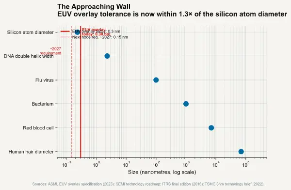
The deviation was 0.4nm. A single strand of human DNA is approximately 2nm in diameter. The tolerance being monitored was tighter than the diameter of a double-helix. This is the frontier at which semiconductor manufacturing now operates — a regime where the physical dimensions being controlled are within an order of magnitude of the atomic scale, where mechanical, thermal, and optical phenomena interact in ways that cannot be fully separated, and where the Tolerance Integration Complexity (TIC) of the manufacturing system exceeds 1,000,000.
Precision as the Engine of the Technology Economy#
The conventional narrative of Moore's Law is one of relentless miniaturisation driven by the ingenuity of circuit designers and the economics of integration. This framing is correct as far as it goes. What it underweights is the mechanical substrate beneath every node transition: the progressive tightening of the dimensional tolerances on which the electrical performance of the circuit depends. Every time a semiconductor company announces a new node, they are not primarily announcing a new circuit architecture — they are announcing that they have achieved and industrialised a new tolerance baseline. The physics of electron transport at 3nm follows from the dimensions; the dimensions follow from the tolerances; the tolerances follow from a supply chain of metrology, materials, and equipment that is among the most concentrated in all of global manufacturing.
The Architecture of Light at 13.5 Nanometres#
From Mercury Lamps to Lasers to Plasma#
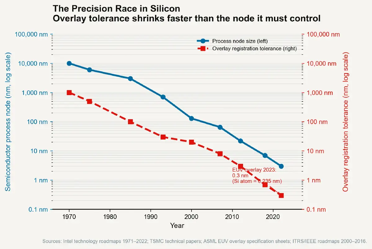
The history of semiconductor lithography is the history of progressively shorter wavelengths of light applied to progressively smaller features. The relationship governing feature size is defined by the Rayleigh criterion: minimum resolvable feature size ≈ k₁ × (λ / NA), where k₁ is a process factor representing the practical minimum for a manufacturable process, λ is the wavelength of the illumination source, and NA is the numerical aperture of the projection lens. To print smaller features, manufacturers must either reduce wavelength, increase numerical aperture, or reduce k₁ — and all three have been pursued simultaneously across the history of the industry.
Mercury arc lamp sources — used from the late 1950s through the 1990s — produced illumination at wavelengths of 436nm (g-line), 405nm (h-line), and 365nm (i-line). Deep ultraviolet excimer lasers (KrF at 248nm, ArF at 193nm) replaced mercury lamps for sub-0.35µm production from the mid-1990s onward. Immersion lithography, introduced in mass production around 2006, placed water between the projection lens and the wafer surface to effectively increase the NA beyond 1.0, enabling 193nm ArF illumination to print features as small as approximately 38nm in single exposure. Multi-patterning — printing a feature set in multiple separate exposures on the same layer — extended the effective resolution further, allowing ArF immersion to reach production at what TSMC designates the 7nm node, where the minimum half-pitch for some layers was approximately 30nm.
EUV lithography at 13.5nm wavelength — approximately 14× shorter than the ArF wavelength — enables single-exposure patterning of features that would require four or five separate ArF multi-patterning steps. The photon energy at 13.5nm (92 eV) is orders of magnitude higher than at 193nm (6.4 eV), which means EUV is absorbed by almost all optical materials. The projection optics must use mirrors operating at grazing or near-normal incidence, polished to surface roughness values of approximately 0.05–0.1nm root-mean-square. A roughness value of 0.1nm is approximately half the diameter of a single carbon atom. Carl Zeiss SMT, the exclusive supplier of the EUV projection optics box for ASML, achieves this surface quality through ion beam figuring and final characterisation using EUV interferometry — a metrology process that is itself at the physical limit of optical measurement.
The Overlay Registration Problem at the Atomic Scale#
A modern integrated circuit is built from 80–130 patterning layers. Each layer's features must be positioned with precise alignment to the features in all previous layers — a requirement called overlay registration. At TSMC's N3 (3nm) node, the overlay specification is approximately ±2nm for critical layers. This means the geometric centre of a feature in the newly exposed layer must fall within 2nm of its intended position relative to the features in the layer below, after all the process steps — deposition, planarisation, etch, cleaning, thermal cycling — that occur between exposures and can shift the wafer's dimensional state.
The ASML NXE:3600D's wafer stage positions the wafer to approximately ±0.1nm using laser interferometry, with the interferometer beam path thermally controlled to approximately ±0.01°C. Silicon's coefficient of thermal expansion is 2.6 parts per million per degree Celsius. A 300mm silicon wafer exposed to a temperature variation of ±0.01°C will expand or contract by approximately ±7.8nm across its full diameter — approximately 4× the overlay budget. The cleanroom temperature environment in which the EUV tool operates is controlled to ±0.05°C, and the wafer is acclimatised to tool temperature before exposure in a conditioning station. The thermal management of EUV production is not an environmental nicety — it is a direct overlay budget contributor.
The EUV light source itself contributes to the overlay budget through focus variation. The EUV plasma source produces pulses of EUV radiation with pulse-to-pulse energy variation of approximately ±0.5%. Each pulse energy variation shifts the focus of the projection optical system slightly — defocus of the projected image produces a position-dependent magnification change that appears as overlay error at the wafer. Correcting this requires real-time focus measurement and adjustment between pulses, using the EUV dose monitor to feed a fast feedback control loop that adjusts the projection optics within each wafer exposure session.
Multi-Patterning and the Tolerance Stack#
For features too fine to print in single EUV exposure — which at N3 includes the most critical metal routing layers — TSMC uses self-aligned multi-patterning (SAMP) processes. A typical self-aligned quadruple patterning (SAQP) sequence involves four sequential lithography and deposition steps, each adding its own overlay registration contribution to the tolerance stack. For four independent overlay registration events, each contributing approximately ±1.5nm uncertainty (at the N3 specification), the combined overlay uncertainty follows the root-sum-square rule: approximately ±3nm total deviation from target at 3σ.
For features whose spacing must be maintained within ±1–2nm from target — which is required at N3 for the most densely packed metal layers — a ±3nm cumulative overlay budget consumes the entire process window. Process engineers allocate the overlay budget across contributors modeled as independent distributions: stage positioning, mask alignment, reticle heating, wafer edge effects, substrate non-planarity. If any single contributor behaves non-independently — for example, a substrate non-planarity that causes systematic overlay shift correlated with previous process step temperature — the root-sum-square model underestimates the tails of the distribution and yield falls.
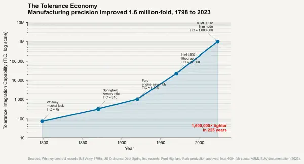
This is where Eli Whitney's tolerance stacking problem manifests at the nanometre scale. Whitney's armourers discovered that when a musket lock required three toleranced components to fit together, the worst-case combination of their tolerances could exceed the allowable fit range. TSMC's process engineers are solving the same problem in a system with millions of toleranced dimensions per chip, where the tolerances are measured in atoms and the consequences of misalignment are quantified in transistor yield maps spanning 900mm² die areas.
What the TIC of 1,000,000 Actually Means#
The TIC for TSMC N3 — the geometric mean of (nominal dimension / tolerance) across all critical feature relationships — exceeds 1,000,000. Stated differently: the precision architecture of a modern leading-edge semiconductor process requires routinely maintaining dimensional accuracy to better than one part in a million of the relevant reference dimension across every critical feature in every one of approximately 80–130 patterning layers on hundreds of thousands of wafers per year, in a production environment.
The historical comparison clarifies the magnitude of this achievement. Eli Whitney's musket lock TIC of approximately 50–100 was considered the frontier of manufacturing precision in 1798. Henry Ford's automotive assembly TIC of 500–2,000 was the frontier of mass production in 1915. The PCB photolithography TIC of 5,000–10,000 was the frontier of electronics manufacturing in 1975. The factor of 10 improvement per industrial generation has produced, over 225 years, a precision infrastructure whose capability would have been physically incomprehensible to the practitioners of each prior era.
The economic architecture supporting TIC of 1,000,000 is correspondingly unprecedented. ASML, the sole supplier of EUV lithography tools, had revenues of approximately $26.3 billion in 2023. Carl Zeiss SMT's EUV optics programme requires approximately 10 years of development time and a manufacturing environment with vibration isolation systems that must attenuate ground motion to submicrometre levels. TSMC's process development cost for each new node exceeds $1 billion before the first wafer reaches a customer. These cost structures are not merely expensive — they represent barriers to entry that have no precedent in industrial history. The precision wall, as it rises, is also a competitive moat. The next post examines where this wall stands now and what the physical limits of EUV overlay registration imply for the semiconductor roadmap beyond 2nm.